research
Nanomaterial based Interfaces for Neural Modulation
 Devices and materials acting as active interfaces to modulate cellular activities is a powerful tool for fundamental studies and for potential non-drug disease treatment. Nanomaterials have been extensively explored for electronics, biological sensing and energy production. Yet, their potential in cell modulation is under studied.
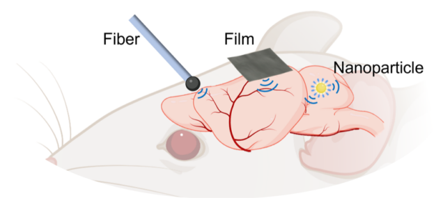
Yang lab has been building built an collaborative research program developing functional nanomaterials and devices to modulate the behavior of cells, especially neurons. We have led the effort inventing various nanomaterial platforms converting laser pulses into localized ultrasound, i.e. photoacoustic effect. These “nanotransducers” have filled an important gap in the neuromodulation field by enabling non-genetic neural stimulation at ultrahigh spatial precision (1 US patent issued, 2 US patent and PCT filed). Our nanomaterial based interface are designed in the form of fiber optoacoustic converters (Nature Communications 2020), tapered fiber optoacoustic emitters (Light Science & Application, 2021), photoacoustic nanotransducers (Matter 2021), photoacoustic biofilm (ACS Nano 2022), and optically drive focused ultrasound (Light Science & Application, 2022). These platforms deliver the high precision neuromodulation in multiple strategies ranging from implantable, injectable to non-invasive ways.
In parallel, we have developed a microwave split ring resonator for high-precision wireless modulation of neuronal activity (US patent and PCT filed) for suppression of seizures in epilepsy and for pain management. Along with innovations, my group also studies the mechanism of microwave neuromodulation and optoacoustic neuromodulation.
Previously, our lab has made substantial scientific contribution in the following area.
Understanding Nano-Cell Interface through Novel Imaging
we have demonstrated a novel label-free imaging in vitro and in vivo imaging graphene oxide, a promising nanomedicine system proposed (Scientific Reports, 5:12394, 2015). We have also demonstrated graphene as a biocompatible protection layer from corrosion for in vivo biomedical devices, for example, to improve success of implants with metal surface (Scientific Reports, doi: 10.1038/srep04097, 2014). Such anti-corrosion film can be significant and broadly needed in many important biomedical applications, such as brain-machine interface which will be studied. We discovered unique intensive and intrinsic nonlinear optical signal of nanowires and applied this property for in vitro and in vivo imaging of silicon nanowires for the first time (Nano Letters, 2009, 9, 2440). We visualized the interaction between nanowires in real time and demonstrated specific targeting of cancer cells (Nano Letters, 2012, 12, 1002). We recently have shown endocytosis of nanowires is through a membrane mechanism, which is one of the first experimental evidences supporting theoretical prediction (Journal of Nanobiotechnology, 15:17, 2017).
Understanding and designing new nanomaterials with unique photonics properties for solar energy applications
We had great interest in understanding and designing nanomaterials with unique physical chemistry properties. We have demonstrated a novel label-free imaging of single wall carbon nanotubes with single tube sensitivity and ability to distinguishing metallic and semiconducting tubes (Physical Review Letters, 105, 217401, 2010) and of graphene with single layer sensitivity (Scientific Reports, 5:12394, 2015) and domain boundary contrast as well as and high speed meeting the large scale production needs (2018).
Nanowires have offered an elegant improvement or solution for addressing solar energy challenges, in photovoltaic, photo electrochemical cells and photosynthesis. Our contribution is to explore semiconductor-metal-semiconductor core-multishell (CMS) nanowires for novel photonic and energy applications such as negative reflective index materials, white LEDs and photoelectrochemical cells. (Scientific Reports, 4:4931, 2014; ACS Photonics, 2018, 5, 5, 1853-1862; Nano Letters, 14, 4517-4522, 2014, Journal of Material Science and Technology, Special issue on 1D nanomaterial, invited review, 2015).
Nanowire architecture for electronics and photonics applications
In the area of novel nanomaterial for nanoelectronics, we have been consistently exploring the ideal nanowire architecture, including new materials, doping, orientation and structural complexity, for large scale, high performance and low power consumption nanoelectronics. We have achieved GaSb (Nano Letters, 15, 4993-5000, 2015) and InSb nanowires, conventionally considered to be fundamental challenging through thin film growth, and pioneered doped GaSb nanowires through the in-situ doping (invited paper, ChemPhysChem, 2012, 13, 2585-2588). We have established the fundamental understanding in controlling the orientation of nanowires in large arrays particularly for two systems, homoepitaxial and heteroepitaxial growth of IV nanowires vertical arrays (Journal of Materials Research, 26, 2744-2748, 2011; Nanomaterials and Nanotechnology, doi: 10.5772/58317 2014) and self-aligned planar growth (Nano Letters, 13, 2786–2791, 2013) and self-catalyzed growth (Nano Letters, DOI: 10.1021/acs.nanolett.6b04046, 2017) of III-V nanowires. My group has demonstrated insights of device physics in core-shell nanowires– a suitable platform for tunneling device applications for low power consumptions (Nano letters, 2011, 11, 1406) and small band gap nanowire devices (Nano Letters, 12, 5331–5336, 2012).